China's Packaging Giants Pour Billions Into New Lines as AI Chips Reshape the Stack
JCET, Tongfu, and Huatian are betting on advanced packaging to capture value downstream of fabrication - and sidestep sanctions that target cutting-edge nodes.
A Quiet Bottleneck Turns Hot
Over the past eighteen months, DailyTechWire has tracked an unmistakable shift in where capital flows inside China's semiconductor ecosystem. While fabrication capacity at sub-7 nm nodes remains constrained by export controls, the segment immediately downstream has become a magnet for investment: chip packaging and testing. In the first half of this year, the country's three largest outsourced assembly houses announced expansion plans that collectively run into the billions of dollars, a spending spree underpinned by double-digit profit growth and a strategic recognition that advanced packaging can unlock performance gains even when process nodes plateau.
Jiangsu Changjiang Electronics Technology, Tongfu Microelectronics, and Huatian Technology - together commanding more than half of China's outsourced assembly capacity - are each racing to add high-density interconnect lines, flip-chip capacity, and heterogeneous integration tooling. The timing is no accident. Artificial intelligence workloads, particularly inference at scale, demand tight integration between compute dies, high-bandwidth memory, and I/O chiplets. Advanced packaging techniques such as 2.5D interposers and through-silicon vias offer a path to close the performance gap when leading-edge lithography is out of reach.
The Economics Behind the Build
Financial tailwinds are making the expansion feasible. According to company disclosures, JCET reported a year-on-year profit increase exceeding 40 percent in the first half, driven by higher utilization rates and a richer mix of automotive and AI-related packaging work. Tongfu and Huatian posted similarly robust figures, each crossing into double-digit net margin territory for the first time in several quarters. The improved profitability reflects two forces: rising average selling prices for advanced packages, and the shift away from commodity smartphone assembly toward higher-value applications in data centers and edge inference modules.
Beijing's policy environment has also tilted decisively in favor of packaging. The third phase of the National Integrated Circuit Industry Investment Fund, colloquially known as the Big Fund III, earmarked substantial allocations for back-end processes, a departure from earlier rounds that prioritized fab construction. Provincial governments in Jiangsu, Sichuan, and Anhui - home to the three giants - have layered on tax incentives and subsidized land leases, effectively reducing the cost of capital for greenfield projects.
What Advanced Packaging Unlocks
For chip designers constrained by node access, packaging has evolved from a cost center into a strategic lever. Chiplet architectures, in which discrete dies are bonded onto a common substrate or interposer, allow companies to mix mature-node logic with cutting-edge memory or analog components. This approach not only improves yield economics but also circumvents export restrictions that apply to monolithic designs fabricated on restricted equipment.
We have seen domestic fabless firms increasingly specify heterogeneous packages in their tape-out roadmaps. One Shenzhen-based AI accelerator startup told industry analysts earlier this year that moving from a single 7 nm die to a multi-chiplet 2.5D package reduced overall silicon cost by nearly 30 percent while improving memory bandwidth by a factor of three. Those gains are difficult to ignore when hyperscalers are procuring inference engines by the tens of thousands.
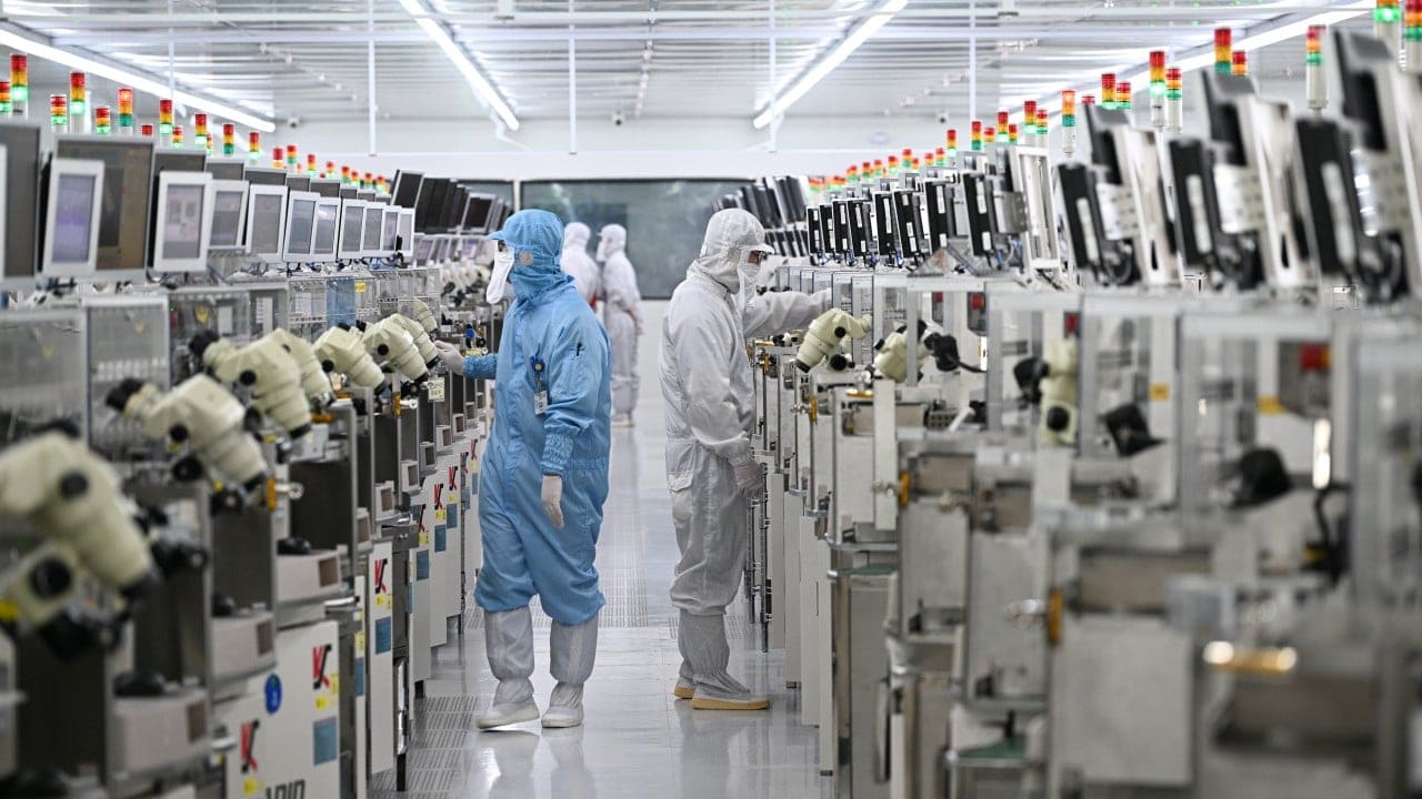
The technical challenges, however, are non-trivial. Advanced packaging requires precision alignment at the micron scale, thermal management across heterogeneous materials, and test protocols that can handle thousands of I/O connections per package. Each of the three companies has invested heavily in metrology and automated optical inspection systems, much of it sourced from European and Japanese toolmakers, to hit the yield and reliability targets that data-center customers demand.
Regional Dynamics and Capacity Distribution
JCET, the largest of the trio by revenue, has concentrated its expansion in Jiangyin and Chengdu, adding flip-chip and wafer-level packaging lines that target automotive radar and AI inference modules. Tongfu is doubling down on fan-out wafer-level packaging in Nantong, a format favored by mobile and edge-AI designers for its thin profile and thermal efficiency. Huatian, historically stronger in discrete and power devices, is pivoting toward system-in-package solutions at its Tianshui and Xi'an sites, aiming to capture share in industrial IoT and automotive control units.
The geographic spread is deliberate. By distributing capacity across inland and coastal provinces, the companies reduce exposure to localized supply-chain disruptions and tap into differentiated labor markets. Chengdu and Xi'an, for instance, offer access to a growing pool of process engineers trained at regional universities, while Jiangyin and Nantong benefit from proximity to Shanghai's logistics hubs and design houses.
Margin Pressure and the Path Forward
Despite the bullish expansion, margin sustainability remains an open question. Advanced packaging lines carry higher depreciation burdens and require continuous yield improvement to stay competitive with Taiwanese and South Korean incumbents. ASE Technology and Amkor, the global leaders, have decades of process refinement and established customer relationships with Intel, AMD, and NVIDIA. Chinese assemblers are still climbing the learning curve, particularly in high-volume production of complex 3D packages.
Pricing dynamics also bear watching. As capacity comes online over the next eighteen to twenty-four months, utilization rates will face downward pressure unless AI demand continues its current trajectory. If inference workloads plateau or if hyperscalers shift toward in-house packaging - a path Amazon and Google have each explored - the market could tip into oversupply, compressing margins and extending payback periods for the new investments.
Regulatory risk layers on additional uncertainty. Export controls have thus far focused on lithography and fab equipment, but packaging tools capable of sub-10 micron bump pitch have drawn scrutiny in recent policy discussions. Any expansion of restrictions to include advanced assembly equipment would force a reordering of supply chains and potentially strand some of the capacity now under construction.
A Bet on the Middle of the Stack
What the expansion ultimately signals is a strategic wager that value in the semiconductor stack is migrating toward integration and heterogeneity. As transistor scaling slows and chiplet ecosystems mature, the ability to co-package disparate functions onto a single module becomes a competitive differentiator. China's assembly giants are positioning themselves at that inflection point, leveraging strong first-half results and policy support to build out capacity before the window narrows.
Whether the bet pays off will hinge on sustained AI demand, continued access to packaging tooling, and the pace at which domestic fabless firms adopt chiplet architectures. For now, the capital is flowing, the lines are going up, and the bottleneck that was once an afterthought is commanding the attention - and the investment - of an entire industry.