Memory Chip Expansion Won't Fix AI Infrastructure Constraints
Microsoft's Azure hardware president argues that brute-force capacity growth misses the deeper supply chain challenges throttling data center deployments across Asia and beyond.

The Capacity Paradox
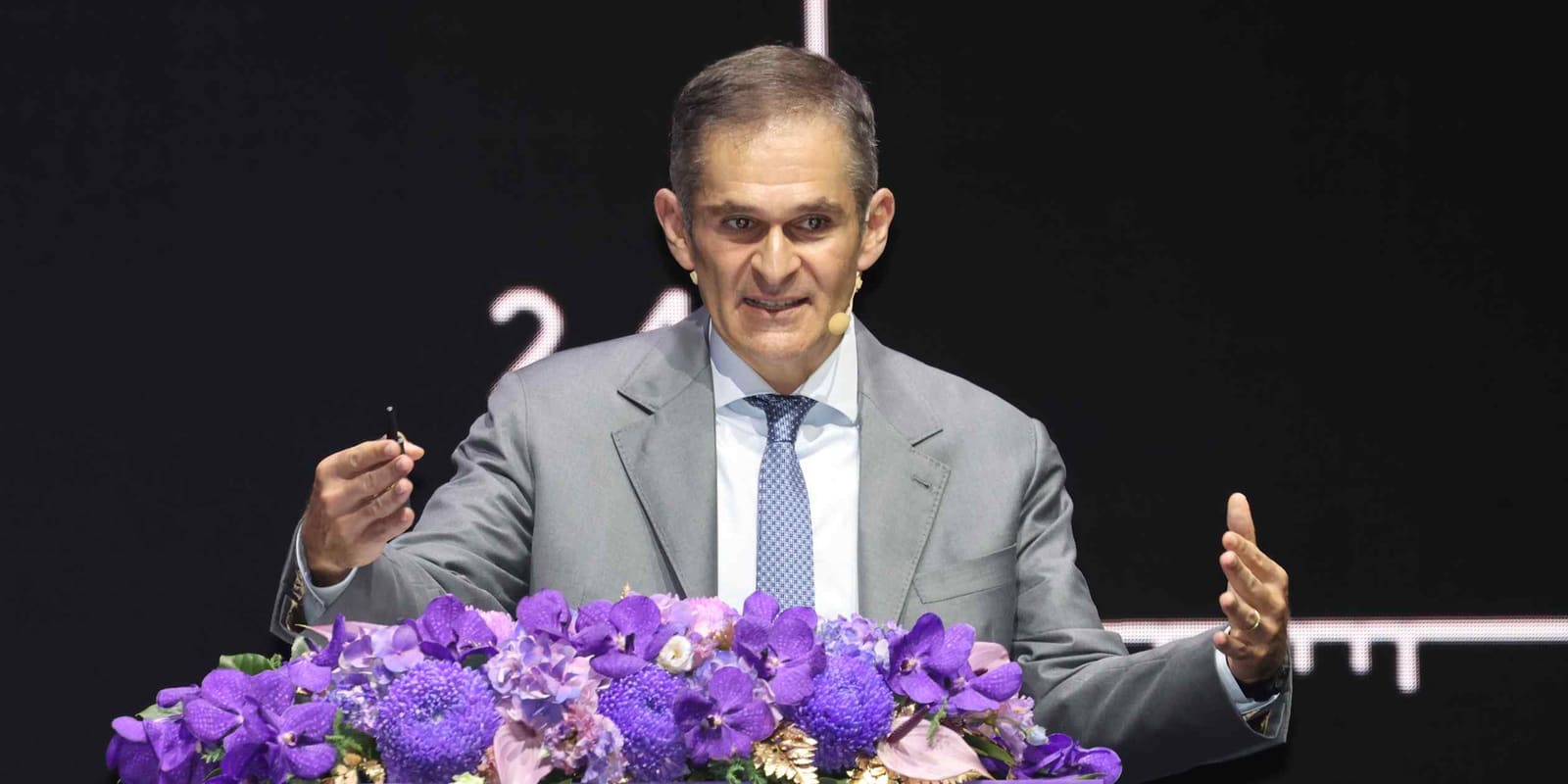
Rani Borkar stood before an auditorium of semiconductor engineers in Taipei this week with a message the industry didn't expect: stop thinking more fabs will solve your problems. As president of Azure Hardware Systems and Infrastructure at Microsoft, Borkar oversees the compute backbone supporting millions of AI workloads daily. Her keynote at SEMICON Taiwan on September 2 challenged the prevailing wisdom that memory chip shortages can be overcome through sheer manufacturing scale.
The bottleneck isn't purely about volume, Borkar argued. Building additional high-bandwidth memory production lines addresses only one variable in a multi-dimensional constraint problem. At DailyTechWire, we've tracked capital expenditure announcements from memory makers across South Korea, Taiwan, and Japan over the past eighteen months. The combined commitments exceed $80 billion through 2027, yet hyperscalers report lead times for advanced packaging and thermal management components stretching to nine months or longer.
Beyond the Wafer
Microsoft's position reflects a shift in how cloud infrastructure leaders are diagnosing supply chain friction. The company operates data centers spanning twenty-eight countries in Asia-Pacific alone, each deployment requiring coordination across dozens of component suppliers. According to Borkar, the real constraints emerge at integration points: interposers that connect memory stacks to GPUs, power delivery networks capable of handling 1,200-watt accelerators, and cooling systems that can dissipate heat densities approaching 100 kilowatts per rack.
Memory chip production has historically followed predictable scaling curves. DRAM and NAND manufacturers invest in new fabs, ramp yields over twelve to eighteen months, and supply stabilizes. That playbook breaks down when the limiting factor isn't the memory die itself but the advanced packaging required to stack eight or twelve DRAM layers into a single HBM3E module. Taiwan Semiconductor Manufacturing Company and Samsung have both expanded their chip-on-wafer-on-substrate capacity, yet packaging remains a choke point industry-wide.
The Innovation Imperative
Borkar's call for innovation rather than capacity echoes concerns we've heard from engineers at Singapore-based data center operators and Bengaluru AI labs. One senior architect at a Southeast Asian cloud provider told us last month that memory bandwidth, not capacity, determines training performance for large language models above 100 billion parameters. Doubling the number of HBM stacks in a system delivers diminishing returns if interconnect latency and power budgets can't scale proportionally.
The Azure hardware chief pointed to alternative approaches: chiplet architectures that reduce reliance on monolithic designs, optical interconnects to replace copper traces at high data rates, and software-level optimizations that compress memory footprints during inference. Microsoft has invested in custom silicon through its Maia AI accelerator family, designed in partnership with TSMC's advanced nodes. Those chips incorporate on-package memory controllers and network interfaces that streamline data movement, reducing the number of discrete components in each server.
Regional Implications
Asia's role in this recalibration is impossible to ignore. South Korea produces the majority of the world's high-bandwidth memory. Taiwan dominates advanced packaging. Japan supplies critical materials for photolithography and chemical mechanical planarization. China, despite export controls on leading-edge equipment, remains a significant player in older-generation DRAM and NAND used in edge AI deployments. Borkar's remarks implicitly acknowledge that no single geography can unilaterally expand capacity fast enough to meet demand projected to grow at 35 percent annually through 2028.
Governments across the region have responded with industrial policy. South Korea's semiconductor support package, announced in March, includes $17 billion in subsidies and tax incentives aimed at memory and logic production. Taiwan's Executive Yuan approved accelerated depreciation schedules for packaging equipment. India's semiconductor mission has attracted proposals for assembly and test facilities, though none yet target HBM-class products. These initiatives address national competitiveness but don't resolve the cross-border coordination failures that delay shipments when a single component is late.
What Engineers Are Watching
Borkar's speech arrives as hyperscalers prepare capital expenditure budgets for 2027. Microsoft, Amazon Web Services, Google Cloud, and Alibaba Cloud have collectively signaled plans to deploy over 2 million AI accelerators in the next two years. Each accelerator requires between six and eight HBM3E stacks, translating to more than 12 million memory modules. SK hynix, the market leader, has guided production to approximately 300,000 wafer starts per month by mid-2027, a figure that implies tight supply even under optimistic yield assumptions.
The technical community is exploring memory architectures that decouple capacity scaling from bandwidth scaling. Processing-in-memory designs, which embed compute logic inside DRAM arrays, reduce data movement and power consumption. Emerging standards like CXL (Compute Express Link) allow memory pools to be shared across multiple processors, improving utilization rates. These innovations require collaboration between chip designers, system integrators, and software developers, a coordination challenge that Borkar suggested is more urgent than raw fab capacity.
The Path Forward
Microsoft's position isn't a dismissal of capacity expansion. The company continues to work with memory suppliers to secure long-term supply agreements and co-invest in R&D for next-generation products. Borkar's argument is that capacity alone is insufficient. The industry must simultaneously innovate on packaging, interconnects, power delivery, and software to unlock the performance gains that AI workloads demand.
For engineers and investors watching the AI infrastructure race, the implication is clear: the next bottleneck is already forming even as the current one eases. Memory chip fabs coming online in 2026 and 2027 will relieve some pressure, but they won't eliminate the fundamental tension between exponential AI model growth and linear improvements in component supply chains. The companies that thrive will be those that optimize across the entire stack, not just the silicon.
Borkar's keynote in Taipei may signal a broader reckoning within the hyperscaler community. Building smarter, not just bigger, is becoming the defining challenge for the next phase of AI infrastructure.