Beijing's Chip Push Accelerates as AMEC Rolls Out Six Production Tools in One Day
The equipment maker's aggressive unveiling signals China's intensifying race to build domestic semiconductor capacity amid export restrictions
A Six-Tool Salvo
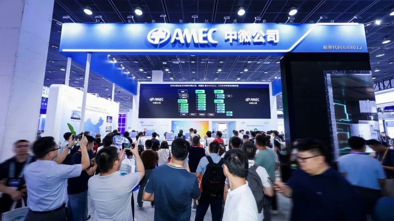
Advanced Micro-Fabrication Equipment (AMEC) introduced half a dozen new chip-making systems at an industry conference in Wuxi this week, a rapid-fire product launch that underscores the urgency Beijing has attached to semiconductor self-sufficiency. The machines, at varying stages of commercial readiness, address multiple steps in wafer fabrication: etching tools that carve nanoscale circuits into silicon, and deposition systems that layer materials atom by atom.
At DailyTechWire, we've tracked how export controls have reshaped capital-equipment roadmaps across the region. AMEC's simultaneous rollout is less a trade-show flourish than a signal of compressed development cycles. When leading-edge lithography and inspection platforms remain out of reach, Chinese fabs need indigenous alternatives for every other process step, and they need them now.
The Equipment Mix
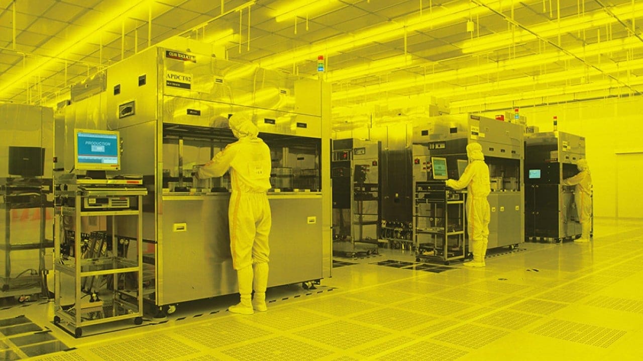
Etching and deposition sit at opposite ends of the pattern-transfer workflow. Etch tools remove material selectively, defining transistor gates, interconnects, and vias. Deposition tools add thin films of metals, dielectrics, and semiconductors. Both require sub-nanometre precision and repeatability across hundreds of wafers per day. AMEC has historically concentrated on plasma etch, where it holds meaningful domestic share; expanding the deposition portfolio suggests the company is chasing a larger slice of the integrated-device-manufacturer tool budget.
The announcement did not specify which nodes the new systems target, but context matters. China's leading fabs are volume-ramping mature processes between 28 nanometres and 14 nanometres, nodes that still demand advanced etch and chemical-vapour-deposition capabilities even if they do not require extreme-ultraviolet lithography. Toolmakers that can deliver high throughput and low defect density at these geometries will capture the capital-expenditure wave rolling through Hefei, Wuhan, and Chengdu.
Policy Meets Production Economics
Beijing's self-reliance mandate has translated into procurement preferences, subsidised financing, and co-development partnerships between equipment vendors and state-backed foundries. That policy tailwind does not guarantee technical success, but it does compress the feedback loop: AMEC can install beta tools in friendly fabs, iterate on chamber design and process recipes, and move to commercial release faster than it could in a purely market-driven environment.
The risk is that speed trades off against yield and reliability. Semiconductor equipment typically undergoes years of qualification before high-volume manufacturing. Accelerated timelines may deliver machines that meet specifications on paper but struggle with uptime, particle contamination, or chamber-matching variability when deployed at scale. Fabs will tolerate higher defect rates if the alternative is no tool at all, but that tolerance has limits, especially as China's device makers chase export markets that demand stringent quality.
The Talent and IP Challenge
Toolmaking is as much about process know-how as hardware. Etch recipes, for instance, balance gas chemistry, radio-frequency power, pressure, and temperature to achieve target profiles without damaging underlying layers. Deposition uniformity hinges on showerhead design, precursor flow dynamics, and thermal management. These details live in the heads of engineers who have spent decades at Applied Materials, Lam Research, and Tokyo Electron.
China has recruited aggressively, offering multiples of Silicon Valley compensation to lure veterans. Some have joined; others have declined, wary of export-control liability or disinclined to relocate. AMEC and its peers have also built partnerships with domestic universities and research institutes, but the pipeline from PhD to production-ready engineer takes years. In the meantime, the company must rely on a smaller bench of experienced process integrators, which constrains how many new platforms it can bring to maturity simultaneously.
Intellectual property remains another friction point. Western equipment vendors hold thousands of patents covering chamber architectures, endpoint-detection algorithms, and plasma-confinement geometries. Designing around that thicket without infringement is possible but time-consuming, and any future attempt to sell tools outside China will invite scrutiny. AMEC has filed its own patent portfolio, but enforceability across jurisdictions is uneven.
Demand Trajectory and Capacity Constraints
Chinese fab capacity is projected to grow by double digits annually through the end of the decade, driven by automotive chips, Internet of Things sensors, power semiconductors, and legacy logic. Each new line requires dozens of etch and deposition chambers. If AMEC can capture even a fraction of that demand, revenue and scale will follow, enabling reinvestment in next-generation platforms.
The constraint is manufacturing capacity for the tools themselves. Semiconductor equipment is low volume and high mix; each chamber is effectively custom-configured for a process step. AMEC must balance production line expansion with quality control, supply-chain resilience for subsystems like vacuum pumps and mass-flow controllers, and field-service coverage as its installed base grows. A six-product launch is a statement of R&D bandwidth; whether the company can ramp production and support at the same pace will determine commercial impact.
What Comes Next
The Wuxi conference unveiling is part of a broader pattern: Chinese tool and materials suppliers front-loading announcements, demonstrating progress to investors, customers, and policymakers. The real test arrives in the quarters ahead, when fabs integrate these systems into production flows and report yield, uptime, and cost of ownership.
For the global equipment industry, AMEC's acceleration is a reminder that export controls create both barriers and incentives. Restricting access to leading-edge tools has slowed China's progress toward sub-7-nanometre logic, but it has also catalysed a parallel ecosystem at mature nodes, one that will eventually compete for share in foundry, power, and analog markets worldwide. The six machines announced this week are data points in that longer arc, and the arc bends toward greater self-sufficiency, even if the path is neither smooth nor guaranteed.