Japan's Chip Comeback Hits $37 Billion as Sony and TSMC Deepen Partnership
Foreign investment in Japanese semiconductor manufacturing reaches new milestone, driven by government subsidies and demand from AI infrastructure players across the region.
A Quiet Milestone in Tokyo's Industrial Strategy
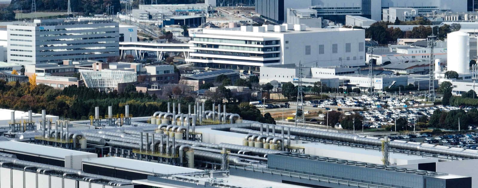
Japan's semiconductor industry just crossed a threshold that would have seemed unlikely five years ago: 6 trillion yen ($37 billion) in foreign investment, according to government tallies. The latest push came from Sony Group and Taiwan Semiconductor Manufacturing Co., which announced plans for an advanced image sensor fabrication facility in Kumamoto prefecture. The plant joins TSMC's two existing foundries in the same region, where the Taiwanese giant has already committed 3 trillion yen.
At DailyTechWire, we've tracked Japan's quiet campaign to rebuild its chipmaking footprint since the first TSMC-Japan discussions surfaced in 2021. What started as a defensive play against supply-chain fragility has evolved into something more ambitious: positioning Japan as a stable, subsidy-backed manufacturing hub for technologies that Seoul and Hsinchu can't easily replicate at scale.
The Image Sensor Bet
Sony and TSMC are targeting image sensors, a category where Japan still holds structural advantages. Sony controls roughly half the global market for CMOS image sensors, components that sit inside every smartphone camera, automotive LiDAR system, and industrial vision module. But leading-edge sensor production requires both Sony's device expertise and TSMC's process control at nodes below 20 nanometers.
The Kumamoto facility will focus on stacked sensor architectures, where logic and pixel arrays are manufactured separately and bonded vertically. These designs improve low-light performance and enable on-chip AI inference, features that matter for autonomous vehicles and next-generation smartphone computational photography. The joint venture structure lets Sony secure leading-edge capacity without building an entire advanced logic fab from scratch, a capital outlay that would strain even its balance sheet.
TSMC's calculus is different. Partnering with Sony gives the Taiwanese foundry a customer anchor in Japan and access to sensor IP that complements its existing logic and analog offerings. It also diversifies TSMC's geographic footprint at a moment when concentration risk in Taiwan remains a boardroom concern across the semiconductor value chain.
Subsidies as Industrial Policy
Tokyo's willingness to deploy fiscal support has been central to this investment wave. The Japanese government has committed subsidies covering up to 40% of eligible capital expenditures for strategic semiconductor projects, a rate that exceeds what most OECD economies offer outside of crisis periods. TSMC's two Kumamoto foundries have drawn several hundred billion yen in state backing; the Sony-TSMC sensor venture is expected to receive similar treatment.
These subsidies work because they target a specific gap. Japan has abundant engineering talent, reliable infrastructure, and proximity to East Asian supply chains, but its domestic semiconductor equipment and materials industries have atrophied since the 1990s. Subsidies lower the entry cost for foreign players who can bring advanced process technology and customer relationships that Japanese firms no longer maintain on their own.
The policy has limits. Subsidies can attract investment, but they don't automatically rebuild ecosystems. TSMC's Kumamoto operations rely heavily on expatriate engineers from Taiwan, and the local talent pipeline remains thin for cutting-edge process integration. Japan's universities produce strong materials scientists and device physicists, but fewer engineers trained in high-volume manufacturing at 7nm and below.
The AI Infrastructure Angle
A second driver, less visible in official announcements, is demand from hyperscale and AI infrastructure customers. U.S. cloud platforms and Asian AI hardware vendors are hunting for diversified manufacturing capacity as they scale out inference accelerators and edge AI modules. Japan offers political stability, strong IP protection, and no immediate risk of export restrictions, a combination that matters when designing multi-year silicon roadmaps.
Image sensors fit this pattern. Advanced sensors are increasingly integrated with neural processing units for on-device computer vision, a design approach that reduces latency and bandwidth costs in edge AI deployments. Automotive customers, particularly those building Level 3 and Level 4 autonomy stacks, want sensors and compute fabbed in regions insulated from cross-strait geopolitical risk. Kumamoto provides that optionality.
TSMC's broader Japan footprint also serves as a hedge. The company's first Kumamoto fab targets 28nm and 22nm nodes, mature processes used in automotive microcontrollers and power management ICs. The second fab, scheduled for volume production in 2027, will handle 12nm and 16nm, nodes that serve 5G radio-frequency front-ends and mid-tier application processors. Adding image sensors to the mix turns Kumamoto into a multi-product site, improving asset utilization and customer stickiness.
Competitive Pressure from Seoul and Shenzhen
Japan's chip resurgence is unfolding against intensifying competition. South Korea and Taiwan recently overtook Japan in semiconductor export value for the first time in decades, driven by memory and AI accelerator shipments. Samsung Electronics is expanding logic foundry capacity in South Korea and exploring partnerships in the U.S. and Europe, directly challenging TSMC's customer base. Meanwhile, Chinese chipmakers continue to push into mature nodes despite U.S. export controls, flooding global markets with low-cost analog and power devices.
For Sony, partnering with TSMC is partly defensive. Samsung manufactures image sensors in-house and has ramped production of sensors for automotive and industrial applications. If Samsung captures meaningful share in those categories, it could leverage vertical integration to bundle sensors with Exynos processors or OLED displays, a strategy Sony can't match without its own advanced logic capacity.
Japan's government sees similar strategic exposure. Without a viable domestic or allied source of leading-edge logic, Japanese electronics and automotive companies would depend entirely on foundries in Taiwan and South Korea, both of which face their own geopolitical and operational risks. The 6 trillion yen in foreign investment is, in effect, Tokyo's insurance premium against supply-chain single points of failure.
What the $37 Billion Buys
The 6 trillion yen figure, while headline-grabbing, obscures important details. Not all of that capital has been deployed yet; much of it represents multi-year commitments tied to construction timelines and subsidy disbursement schedules. TSMC's two Kumamoto fabs account for roughly half the total, with the Sony-TSMC image sensor venture adding another significant tranche. Smaller investments from equipment suppliers and materials companies make up the remainder.
Still, the aggregate number signals a shift. Japan is no longer a tertiary option for semiconductor manufacturing. For technologies where process maturity, supply-chain proximity, and political risk matter more than absolute cost, Japan is back in the conversation.
The harder question is whether this investment wave translates into sustained competitiveness. Subsidies can bootstrap an industry, but they don't guarantee long-term viability. Japan's challenge is to convert these initial foreign commitments into a self-reinforcing ecosystem: local talent development, domestic equipment innovation, and customer demand that justifies continued capital allocation.
Looking Ahead
At DailyTechWire, we see Japan's semiconductor strategy as part of a broader regional rebalancing. As the U.S., Europe, and East Asian governments all pursue some version of chip sovereignty, manufacturing capacity is fragmenting along geopolitical lines. Japan's advantage is that it sits inside the U.S.-allied technology bloc while maintaining deep commercial ties across Asia.
The Sony-TSMC image sensor venture is a test case. If the partnership delivers competitive products on schedule and attracts follow-on investment from automotive and AI customers, it will validate Tokyo's subsidy-driven approach. If execution stumbles or demand shifts elsewhere, Japan risks becoming a high-cost manufacturing outlier propped up by fiscal support that can't last indefinitely.
For now, the $37 billion milestone is a data point, not a verdict. The real measure will be whether these fabs are still running at healthy utilization rates five years from now, and whether Japanese engineers are leading the next generation of process and device innovation. That outcome is far from guaranteed, but the pieces are in place for Japan to reclaim a meaningful role in the global semiconductor industry.