China's Memory Champion Bets on Low-Power Chip Path
A venture arm linked to YMTC has invested in SOI Micro, a domestic player pursuing fully depleted silicon-on-insulator technology as Beijing seeks alternatives to cutting-edge lithography.
A Strategic Pivot in China's Semiconductor Playbook
When export controls tightened around extreme ultraviolet lithography and high-end process nodes, Beijing's semiconductor industry began exploring roads that do not require the most restricted tools. One of those roads is fully depleted silicon-on-insulator technology, and it just gained a heavyweight financial backer: a venture fund tied to Yangtze Memory Technologies, the country's largest NAND flash producer.
The fund has taken a position in SOI Micro, a domestic chipmaker specializing in FD-SOI fabrication. The deal signals that China's established memory players see strategic value in technologies that offer competitive power efficiency and performance without pushing into the sub-3-nanometer territory that demands EUV scanners.
At DailyTechWire, we have tracked similar moves across the region over the past eighteen months. While Seoul and Taiwan have poured capital into advanced FinFET and gate-all-around architectures, mainland manufacturers have quietly assembled a portfolio of alternative node strategies, from mature-node capacity expansion to specialized process flows like FD-SOI.
What FD-SOI Brings to the Table
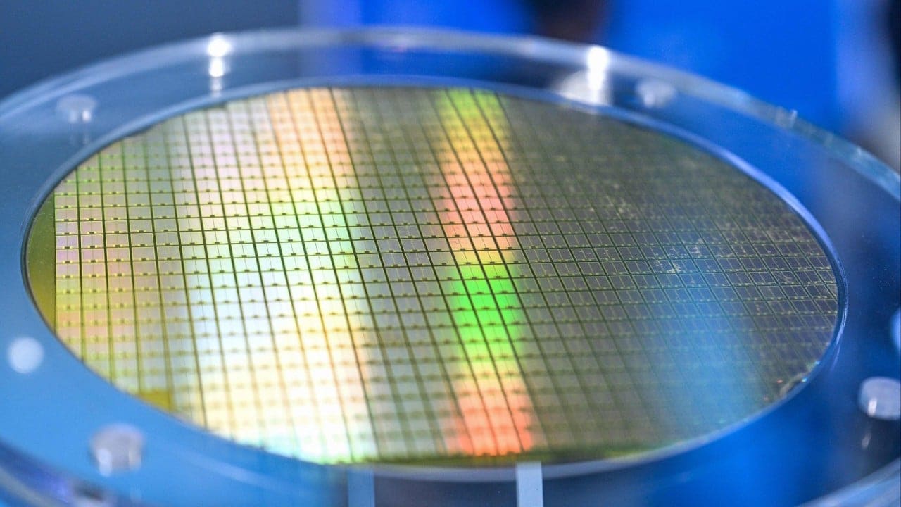
Fully depleted silicon-on-insulator is not a new idea. The approach places a thin silicon layer atop an insulating substrate, reducing parasitic capacitance and leakage current. The result is lower power consumption at comparable or even superior performance levels for certain applications, particularly in edge compute, automotive controllers, and Internet of Things endpoints where battery life and thermal budgets matter more than raw gigahertz.
Unlike FinFET or gate-all-around transistors, FD-SOI can be manufactured on 28-nanometer and 22-nanometer nodes using deep ultraviolet lithography, the workhorse tool that remains widely available and unencumbered by the most restrictive export rules. That makes it an attractive hedge for any fab operator navigating the current geopolitical landscape.
The technology also simplifies back-biasing, a technique that dynamically adjusts transistor threshold voltage to balance speed and power on the fly. For mobile processors, wearables, and sensor hubs, that tunability translates into longer runtime and cooler operation, two attributes that matter as much as peak throughput in many real-world deployments.
Why a Memory Giant Cares About Logic
YMTC is best known for 3D NAND, a category where it has made significant strides in stacking layers and closing the gap with incumbents. Investing in a logic-focused FD-SOI player might seem tangential, but the rationale becomes clearer when viewed through the lens of vertical integration and ecosystem resilience.
Modern memory controllers, interface chips, and power-management ICs all benefit from low-leakage logic. As YMTC scales its NAND output, it will need more of those ancillary components, and sourcing them domestically reduces supply-chain risk. By backing SOI Micro, the venture fund positions itself to influence the development of complementary chips that can be co-packaged or integrated alongside memory dies.
There is also a talent and know-how dimension. FD-SOI requires expertise in substrate engineering, radio-frequency design, and analog-digital mixed-signal layout, skills that overlap with the requirements for next-generation memory architectures like compute-in-memory and near-data processing. Cross-pollination between the two domains could accelerate innovation in both.
The Competitive Landscape and Regional Context
SOI Micro is not operating in a vacuum. Globally, FD-SOI has found its strongest champion in European fabs, where the technology has been deployed for automotive and industrial applications. In Asia, adoption has been more selective, with most leading-edge investment flowing into FinFET and more recently into nanosheet and nanowire gate structures.
Yet the calculus is shifting. As the cost of each new process node climbs and the performance gains narrow, more design teams are reconsidering whether chasing the bleeding edge makes economic sense for every product category. FD-SOI offers a middle path: better power efficiency than planar bulk silicon, lower mask costs than FinFET, and a mature supply chain that does not depend on a handful of controlled chokepoints.
For China specifically, the technology aligns with policy priorities. Domestic semiconductor roadmaps emphasize self-sufficiency in mature and specialty nodes, and FD-SOI fits squarely in that envelope. It also plays to the strengths of local equipment suppliers, who have made faster progress in DUV than in EUV or advanced packaging.
Implications for the Broader Chip Ecosystem
The involvement of a fund linked to a leading memory manufacturer underscores a broader trend: China's semiconductor industry is no longer betting on a single process node or architectural paradigm. Instead, it is assembling a mosaic of capabilities, each optimized for different markets and regulatory environments.
This portfolio approach has parallels in other technology domains. In AI accelerators, Chinese firms have pursued both training-class GPUs and inference-optimized ASICs. In connectivity, investments span sub-6 GHz 5G, millimeter-wave components, and satellite communication modules. The common thread is diversification, a hedge against the risk that any single technology path becomes inaccessible or uncompetitive.
For global chip buyers, the rise of alternative node strategies introduces both opportunity and complexity. On one hand, more process options mean more potential suppliers and price competition. On the other, it complicates qualification and ecosystem support, especially when different regions converge on incompatible standards or toolchains.
What to Watch Next
SOI Micro's ability to scale production and win design wins outside captive customers will be the first test. FD-SOI has historically struggled to gain traction in high-volume consumer markets, where the installed base of FinFET design IP and the inertia of existing supply chains create formidable barriers. Automotive and industrial segments offer a more receptive audience, but they also demand rigorous reliability and long product lifecycles, which require sustained investment in process maturity.
The venture fund's participation may also signal future M&A or partnership activity. If YMTC or its affiliates see strategic value in tighter integration between memory and logic, an outright acquisition or joint-venture fab could follow. Such moves would mirror patterns elsewhere in Asia, where vertical integration has become a key lever for competitiveness.
Finally, the geopolitical dimension remains fluid. Export control regimes are dynamic, and technologies that seem unencumbered today may face new restrictions tomorrow. The fact that FD-SOI relies on DUV rather than EUV offers some insulation, but it is not absolute. Any expansion of controls to cover substrates, precursor chemicals, or metrology tools could reshape the calculus once again.
For now, the investment marks another data point in China's patient, multi-threaded approach to semiconductor resilience. It is a reminder that in an industry where the cutting edge captures most of the headlines, the real competitive advantage may lie in mastering the alternatives.