China's Chipmaking Push Extends to Wafer Polishing as Hwatsing Unveils Metrology Tool
A six-inch wafer measurement system marks progress in domestic semiconductor equipment, though advanced lithography remains out of reach
Incremental Gains in a Strategic Sector
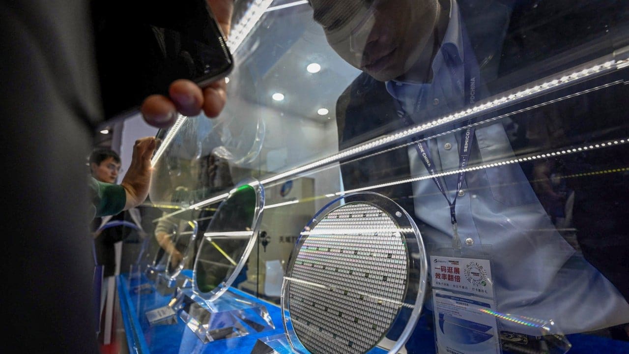
China's semiconductor equipment makers are notching wins in corners of the chipmaking process that rarely capture headlines. Hwatsing Technology, the country's largest supplier of chemical mechanical polishing (CMP) tools, introduced a metrology system for six-inch wafers this week. The system measures surface flatness and smoothness with nanometer-level precision, a capability essential for ensuring that polished silicon discs meet the exacting tolerances required by subsequent fabrication steps.
At DailyTechWire, we've tracked the steady drumbeat of announcements from Chinese toolmakers over the past eighteen months. Each represents a small piece of a much larger puzzle: building a domestic supply chain capable of supporting advanced semiconductor production without relying on equipment from ASML, Applied Materials, Tokyo Electron, and other foreign giants. Wafer polishing sits downstream from lithography and deposition, but its importance is no less real. Without uniform, defect-free surfaces, chips fail at higher rates and yields plummet.
What Chemical Mechanical Polishing Does
CMP is a hybrid process that combines chemical slurry with mechanical abrasion to flatten wafer surfaces between fabrication layers. Modern logic and memory chips stack dozens of metal and dielectric layers; each must be planarized before the next is deposited. The metrology component measures topography in real time, feeding data back to the polishing tool so that pressure, slurry flow, and pad rotation can be adjusted on the fly.
Hwatsing's new system targets six-inch wafers, a format still used in power semiconductors, analog ICs, and certain MEMS devices. The company has not disclosed whether the metrology platform will scale to twelve-inch wafers, the industry standard for leading-edge logic and DRAM. Six-inch tooling serves niche markets and legacy fabs, but it also provides a proving ground for subsystems that may later migrate to larger formats.
The Broader Equipment Landscape
China's chipmaking ambitions rest on two parallel tracks: expanding production capacity and localizing the equipment that fills those fabs. Export controls introduced by the United States, the Netherlands, and Japan over the past three years have restricted access to extreme ultraviolet lithography systems, high-end dry etch tools, and advanced deposition equipment. Those restrictions have accelerated investment in domestic alternatives, even when the alternatives lag by a generation or more.
Polishing equipment occupies a middle tier of complexity. It does not require the sub-nanometer precision of EUV optics or the plasma chemistry expertise of atomic layer deposition, but it demands tight integration of sensors, control algorithms, and consumables such as pads and slurries. Hwatsing has been building CMP tools for more than a decade, initially serving mature-node fabs and gradually moving upmarket. The company's tools are now deployed in several Chinese memory and logic facilities, though foreign suppliers still dominate at the leading edge.
Why Metrology Matters
Measurement is as critical as the process itself. A polishing tool that cannot verify its own output in real time risks sending defective wafers into subsequent steps, where the cost of failure rises exponentially. Inline metrology reduces cycle time and improves yield by catching deviations before they propagate. Hwatsing's announcement suggests that the company is moving beyond simple process control toward closed-loop systems that adjust parameters dynamically.
The six-inch format limits immediate commercial impact, but it signals technical capability. If Hwatsing can deliver metrology that meets the precision requirements of power and analog fabs, the technology may prove adaptable to twelve-inch platforms used in high-volume manufacturing. The company has not disclosed accuracy specifications or benchmarked the system against tools from KLA or Onto Innovation, the established leaders in semiconductor metrology.
Lithography Remains the Chokepoint
Polishing progress does not change the central constraint facing China's chip industry: access to advanced lithography. ASML's EUV systems, which pattern features smaller than seven nanometers, are subject to export restrictions that show no sign of loosening. China's most advanced domestic lithography tool, developed by Shanghai Micro Electronics Equipment, operates at 28-nanometer resolution and uses deep ultraviolet light. That places it roughly two decades behind ASML's state of the art.
Without EUV, Chinese fabs cannot manufacture the processors and AI accelerators that power frontier models and hyperscale data centers. They can, however, produce a wide range of chips for automotive, industrial, and consumer applications, where 28-nanometer and older nodes remain cost-effective. Polishing, deposition, and etch tools that serve those nodes represent a pragmatic target for localization efforts.
Regional Investment Patterns
Semiconductor equipment development in China is funded through a mix of state-backed investment funds, provincial incentives, and private capital. Hwatsing has received support from the National Integrated Circuit Industry Investment Fund, known colloquially as the Big Fund, which has deployed tens of billions of dollars across the supply chain since 2014. The second phase of the fund, launched in 2019, prioritized equipment and materials over fab construction, reflecting a strategic shift toward reducing foreign dependencies at the tool level.
The company is based in Shenyang, in northeastern China, a region with a smaller concentration of semiconductor activity than the Yangtze River Delta or the Pearl River Delta. Its location reflects the geographic dispersion of China's equipment industry, which spans multiple provinces and competes for talent with established hubs in Shanghai, Beijing, and Shenzhen.
What Comes Next
Hwatsing's metrology system will enter pilot production lines over the next several quarters. Success will be measured not by announcements but by adoption rates in commercial fabs, where yield and uptime determine whether a tool displaces an incumbent. Chinese chipmakers face pressure to buy domestic equipment when feasible, but they also operate under margin constraints that leave little room for underperforming tools.
The trajectory for Chinese semiconductor equipment is one of gradual capability building rather than sudden breakthroughs. Polishing is one of many process steps that must be mastered. Each incremental gain reduces reliance on foreign suppliers and expands the addressable market for domestic toolmakers. The gap remains wide, but the direction of travel is clear.