The Chip Tool Everyone Wants: TSMC, Samsung and Intel Race to Deploy High NA EUV
ASML's next-generation lithography machine has become the new battleground in semiconductor manufacturing, with deployment timelines revealing strategic priorities across three giants.
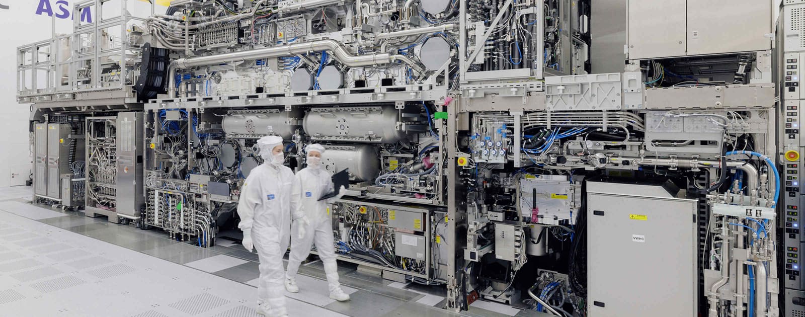
A New Lithography Divide
The world's three leading foundries have staked out markedly different positions on when they will adopt ASML's high numerical aperture extreme ultraviolet lithography machines, with deployment timelines spanning from immediate use to four years out. Taiwan Semiconductor Manufacturing Company announced on 8 September that it will begin mass production using high NA EUV systems in 2030, according to the company. Samsung Electronics is targeting adoption as early as 2028, whilst Intel has stated it is already producing chips at volume with the technology.
At DailyTechWire, we have tracked capital equipment races before, but rarely has a single tool category prompted such public jockeying over deployment schedules. The divergence reflects not just engineering readiness but also distinct bets on where process advantage will matter most over the next half-decade.
What High NA EUV Unlocks
High NA EUV lithography systems represent the cutting edge of chipmaking equipment. These machines use light with a wavelength of 13.5 nanometres to pattern features on silicon wafers, but the new high NA variant increases the numerical aperture of the optical system from 0.33 to 0.55. That jump allows finer patterning resolution, enabling chipmakers to print smaller transistor features without resorting to multiple exposures or complex workarounds.
The practical upshot is denser logic and memory arrays, lower power consumption per transistor, and the ability to push Moore's Law economics further before hitting the next physics wall. ASML, the sole supplier of EUV lithography equipment, has priced each high NA system well above 300 million euros, making them the most expensive production tools in semiconductor manufacturing.
For foundries chasing leadership in artificial intelligence accelerators and high-performance compute, high NA EUV is the gateway to sub-two-nanometre nodes and the transistor densities those nodes promise.
TSMC's 2030 Timeline and the Calculus of Caution
TSMC's decision to target 2030 for mass production use is the most conservative of the three. The Hsinchu-based manufacturer, which commands more than 60 per cent of global foundry revenue, has built its dominance on process stability and yield rather than racing to deploy immature toolsets.
A 2030 start date suggests TSMC believes its existing EUV systems and multi-patterning techniques can carry it through the next node transitions without sacrificing competitiveness. The company is expected to bring its two-nanometre process into volume production in 2025 and its so-called A16 node, which incorporates backside power delivery, around 2026 or 2027. High NA EUV would likely slot into the generation beyond that, possibly coinciding with a sub-1.5-nanometre node.
The timeline also reflects capital discipline. TSMC has committed to capital expenditure in the range of 28 billion to 32 billion US dollars annually in recent guidance, and high NA tools will consume a disproportionate share of any lithography budget. Delaying deployment allows the toolmaker to refine the technology and for TSMC to extract maximum return from its installed base of standard EUV scanners.
Yet the approach carries risk. If customers, particularly hyperscalers designing their own AI chips, begin to perceive a process disadvantage relative to rivals deploying high NA earlier, TSMC could face margin pressure or design win losses in the most lucrative segment of the market.
Samsung's 2028 Ambition
Samsung's 2028 target sits between TSMC's caution and Intel's claimed head start. The South Korean conglomerate has been vocal about its ambition to reclaim foundry leadership, and early adoption of high NA EUV fits that narrative.
Samsung's foundry business has struggled with yield issues on its three-nanometre and four-nanometre processes, leading some customers to shift orders back to TSMC. A successful deployment of high NA EUV in 2028 would allow Samsung to leapfrog in marketing messaging, even if actual volume ramps lag the announcement by quarters.
The 2028 date also aligns with Samsung's roadmap for what it calls its 1.4-nanometre node, which the company has indicated will rely on gate-all-around transistor architectures and advanced lithography. Whether Samsung can execute on that schedule without repeating the yield stumbles of recent nodes will determine if the high NA investment translates into competitive advantage or expensive distraction.
Intel's Present-Tense Claim
Intel's assertion that it is already mass producing with high NA EUV is the most aggressive statement of the three. The US chipmaker has positioned its so-called Intel 18A process, expected to enter volume production in late 2025 or early 2026, as a technology showcase for both internal products and external foundry customers.
If Intel is indeed running high NA tools in production today, it would represent a significant lead in learning curve and process integration. However, the definition of mass production matters. Early production volumes on new tools are often constrained by tool count, uptime, and throughput, and it is unclear whether Intel's current use constitutes true high-volume manufacturing or pilot-scale production ahead of a broader ramp.
Intel has bet heavily on process leadership as the foundation of its foundry ambitions under chief executive Pat Gelsinger. The company has committed to deploying five process nodes in four years and has secured billions in subsidies from the US government to build fabs in Arizona, Ohio, and New Mexico. High NA EUV is central to that roadmap, and any stumble in yield or cost would reverberate across Intel's entire turnaround strategy.
The Geopolitics Beneath the Tools
The race to deploy high NA EUV is not purely a technical or commercial contest. ASML's monopoly on EUV lithography has made the company a focal point in semiconductor export controls, particularly those targeting China. The Dutch government, under pressure from the United States, has restricted ASML from shipping even older-generation EUV systems to Chinese customers.
High NA tools are subject to even tighter restrictions, effectively ensuring that only manufacturers in allied nations can access them. That dynamic reinforces the bifurcation of the global chip supply chain and raises the stakes for TSMC, Samsung, and Intel. Whichever foundry can master high NA manufacturing first will not only gain a process edge but also solidify its position as the partner of choice for Western governments and hyperscalers wary of geopolitical risk.
China, meanwhile, is pursuing indigenous EUV development, but most analysts believe a domestic high NA equivalent remains a decade or more away. The technology gap is widening, and high NA EUV is the sharp end of that divergence.
What the Timelines Reveal
The spread in deployment dates, from Intel's current use to TSMC's 2030 target, tells a story about risk tolerance, capital strategy, and competitive positioning. Intel is betting that early leadership on a difficult tool will translate into foundry credibility. Samsung is betting that a middle path can deliver marketing advantage without overextending. TSMC is betting that its customers value yield and reliability over the prestige of the newest machine.
All three are likely correct within their own contexts. The question is whether the AI boom, which has driven unprecedented demand for leading-edge logic, will reward the first mover or the most disciplined operator. The answer will shape not just market share but the balance of semiconductor power for the rest of the decade.